When it comes to semiconductor fabrication or any process where contamination is catastrophic, the choice of piping system is a fundamental engineering decision. UHP and HP piping are often used interchangeably. They are not the same – and confusing them can mean costly defects.
What Is High Purity (HP) Piping?
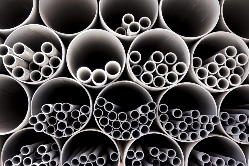
High Purity piping transports gases and liquids with minimal contamination. HP systems use higher-grade materials — typically 316L stainless steel – manufactured and installed under controlled conditions, cleaned before installation to remove grease and particulates.
HP piping is used in biotech, food and beverage, specialty chemicals, and general cleanroom environments: settings where purity matters, but contamination tolerances are not as extreme as in semiconductor fabrication.
HP piping characteristics:
- Material: 316L stainless steel (ASTM A270 or equivalent)
- Surface finish: Mechanically polished to ~20–25 Ra microinch
- Joining: Orbital welding or hygienic fittings
- Cleaning: Cleaned and capped at the factory, passivated on-site
What Is Ultra-High Purity (UHP) Piping?
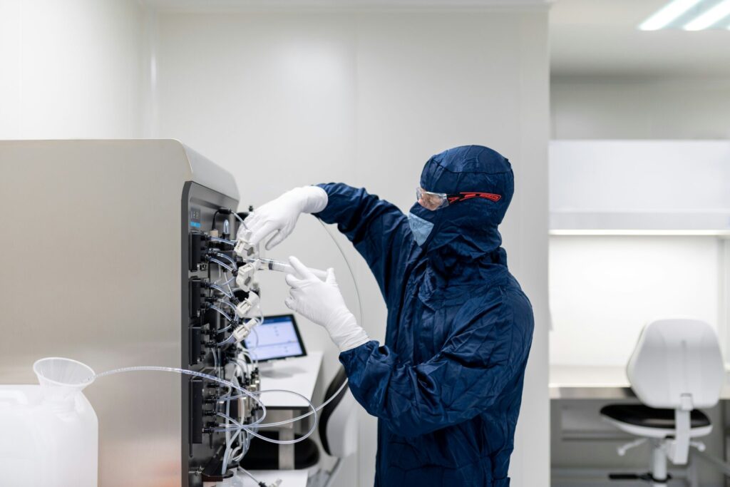
UHP piping takes every aspect of HP construction further. These systems are designed for environments where even parts-per-trillion of contamination can destroy a semiconductor device. Wafer fabrication is the most demanding user of UHP piping.
UHP piping characteristics:
- Material: 316L stainless steel with tightly controlled alloy chemistry, or fluoropolymers for specific chemistries
- Surface finish: Electropolished to ≤10 Ra microinch – some specs require 5 Ra or below
- Joining: Fully automated orbital welding with inert gas purging on both sides
- Internal cleanliness: Cleaned, passivated, and nitrogen-bagged in a controlled environment — never exposed to ambient air post-clean
- Documentation: Full material traceability, weld logs, boroscope records, and certificates of conformance for every component
HP vs UHP: What Actually Changes
UHP takes HP construction and changes five things. The surface finish goes from mechanical polish to electropolished. Welding becomes fully automated. Purging moves from single-side to dual-side inert gas. Post-clean packaging switches to nitrogen-bagging. And documentation scales up to full SEMI traceability. Each change exists because the consequences of contamination in semiconductor fabrication are severe enough to justify it.
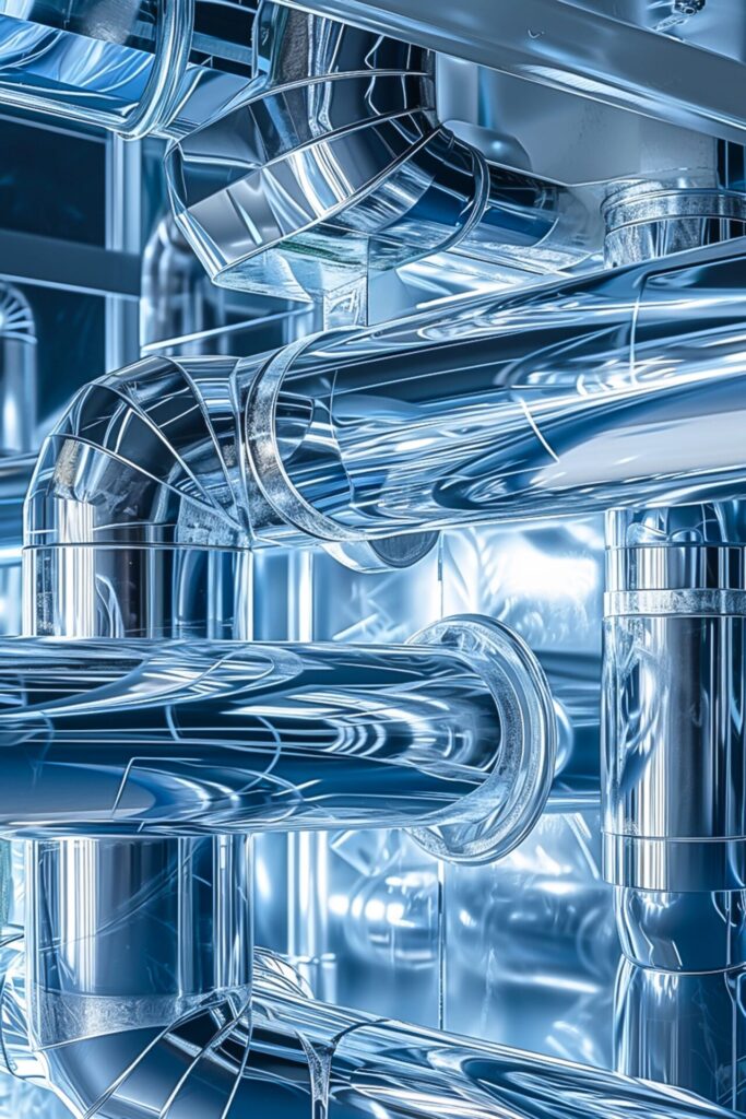
Why Surface Finish Is the Critical Differentiator
A rougher surface has more microscopic peaks and valleys where particles and moisture can adhere and later release into the process stream. In semiconductor processes — where a single stray particle can kill a chip – this is unacceptable.
Electropolishing removes a thin, controlled layer of metal from the internal surface, eliminating micro-asperities and creating a chromium-oxide-rich passive layer that resists corrosion and minimises particle generation. This is why electropolishing is a specification requirement in UHP piping, not an optional upgrade.
When Do You Need UHP Instead of HP?
Ask four questions. What is your contamination tolerance – parts-per-trillion or parts-per-million? What are you transporting – specialty gases like silane or hydrogen fluoride, or lower-sensitivity fluids? Which industry standard governs your facility -SEMI F20 for semiconductor, or ASME BPE for pharma? And what does a contamination failure actually cost? In a cutting-edge fab, a single event can cost millions. The additional investment in UHP is risk management, not a luxury.
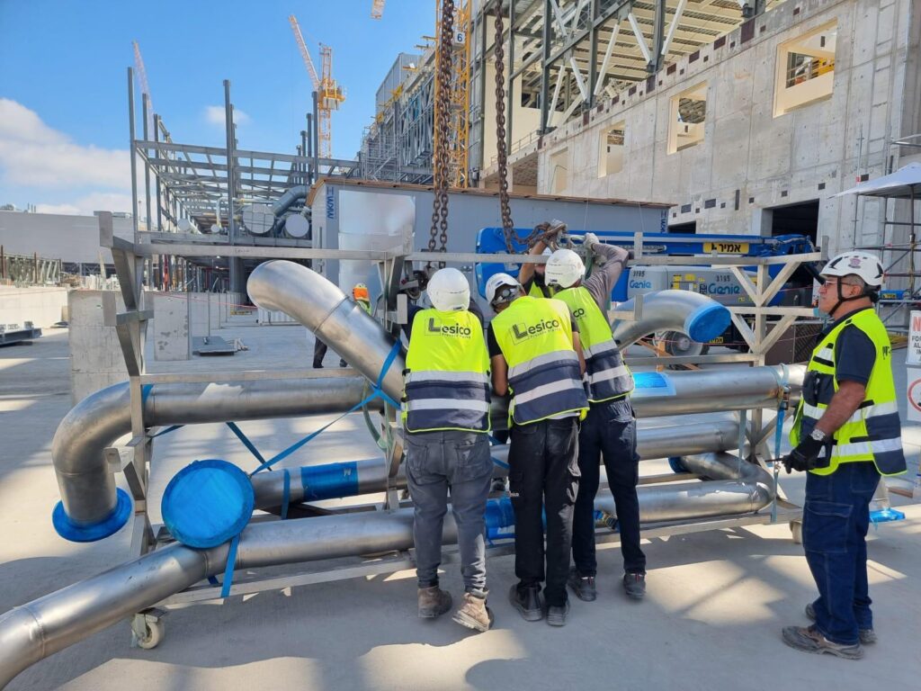
How Lesico Designs and Fabricates UHP and HP Systems
At Lesico, we design and fabricate both HP and UHP piping systems for semiconductor fabs and advanced technology facilities across Europe and beyond. Our off-site manufacturing approach means fabrication happens under controlled conditions – with full weld documentation and material traceability – before a single pipe section reaches your cleanroom.
Planning a UHP or HP piping project? Talk to the Lesico engineering team.